hierarchical building blocks

While it is technically possible to build a general purpose digital computer using NAND gates alone, the logistics of such a task would be unmanageable.

A microcomputer chip such as the Motorola 68000 device comprising the equivalent of some 70 thousand gates would require some 17,500  integrated circuit packages.  Besides 17,500 power and 17,500 ground connections have to be made and some 210,000 pins have to be interconnected.

Furthermore, each 7400 package would draw about 12 milliamperes and the total system would draw 210 amperes at 5 volts consuming in excess of 1 kilowatt of energy.

The 800 milliampere-hour cells of the type used in the Digital Lab Kit would run such a computer built using only 7400 NAND gates for no more than 15 seconds if at all it is possible to draw 210 amperes from these cells.

We attack this problem by looking at combination of gates as combinatorial circuits as the next level above gates along the path to building the computer using hierarchical design and (computer aided) design tools.


combinational circuits

Combinatorial circuits comprise logic gates whose outputs at any time are determined by combining the values of the applied inputs using logic operations.  If there are n input variables

  • there are 2n possible binary input combinations
  • there are 2n entries in the truth table for each output

We can look at the system not in terms of gates but in terms of combinational circuits comprising gates connected together to carry out common useful functions.


hierarchical design

The specification of the building blocks can take many forms -- from equivalent gate level combinational circuits (d) to functional black boxes (a)

In the hierarchical description in terms of actual blocks (a) and in terms of re-usable blocks (b).

Hierarchy has three important properties

  1. reduces complexity required to represent the circuit
  2. ends up with leaf cells upon which the system is built
  3. blocks are universal and reusable at different levels

analysis procedure

The analysis of combinational circuits enables us to determine the functions that the circuits implement.

Boolean functions

First ensure that the circuit is combinational, that is it is free of feedback of an output to an input that the output depends on.

  • label all inputs -- input variables
  • label all outputs -- output functions
  • label all intermediate signals (outputs that feed inputs)

For each output functions, write it in terms of its input variables and intermediate signals, and then expand intermediate signals until the outputs are expressed only in terms of the inputs.

truth tables

Truth tables can be derived directly from the Boolean functions, or by means directly working out from the circuit the outputs for each possible combination of inputs.

X
Y
Z
C
_
C
T1
T2
T3
S
0
0
0
0
1
0
0
0
0
0
0
1
0
1
0
1
1
1
0
1
0
0
1
0
1
1
1
0
1
1
1
0
0
1
0
0
1
0
0
0
1
0
1
1
1
1
0
1
1
0
0
1
0
0
1
1
0
1
0
0
1
0
0
1
1
1
1
0
1
1
0
1

Note that the output of the carry, C, is given by majority function -- that is C is a 1 when the majority (at least 2) of the three inputs, X, Y and Z is 1.


design procedure

The design procedure for combinational circuits is in many ways the reverse of the analysis procedure.  It starts at the problem specification and comprises the following steps:

  1. determine required number of inputs and outputs from the specifications
  2. derive the truth table for each of the outputs based on their relationships to the input
  3. simplify the Boolean functions for each output as a function of its inputs
  4. draw a logic diagram that represents the implementation of the design

The verification of the design is by analysis of its implementation.  The example below shows the steps in the design of a binary adder where F is the sum of X, Y and Z.


BCD to excess-3 code converter

decimal BCD input excess-3 output
A B C D W X Y Z
0 0 0 0 0 0 0 1 1
1 0 0 0 1 0 1 0 0
2 0 0 1 0 0 1 0 1
3 0 0 1 1 0 1 1 0
4 0 1 0 0 0 1 1 1
5 0 1 0 1 1 0 0 0
6 0 1 1 0 1 0 0 1
7 0 1 1 1 1 0 1 0
8 1 0 0 0 1 0 1 1
9 1 0 0 1 1 1 0 0

We start with the truth table for the code converter.

From the K-maps, we can reduce the expressions for each of the outputs to minimal sum of products.

W = A + B C + B D           = A + B(C + D)
    _     _       _ _         _            _ _
X = B C + B D + B C D       = B(C + D) + B C D 
          _ _                 _______
Y = C D + C D               = C XOR D
    _
Z = D

Unlike in the case of minimisation for a single output, the alternative form of the expressions with further factorisation of the term (C + D) allow for the sharing of the circuits in this case.  The penalty however is increased delay because there are more gates in series between the inputs and outputs.


BCD to seven segment decoder

BCD input seven segment decoder
A B C D a b c d e f g
0 0 0 0 1 1 1 1 1 1 0
0 0 0 1 0 1 1 0 0 0 0
0 0 1 0 1 1 0 1 1 0 1
0 0 1 1 1 1 1 1 0 0 1
0 1 0 0 0 1 1 0 0 1 1
0 1 0 1 1 0 1 1 0 1 1
0 1 1 0 1 0 1 1 1 1 1
0 1 1 1 1 1 1 0 0 0 0
1 0 0 0 1 1 1 1 1 1 1
1 0 0 1 1 1 1 1 0 1 1
all other inputs 0 0 0 0 0 0 0

The specification above requires that the output be zeroes (none of the segments are lighted up) when the input is not a BCD digit.  In practical implementations, this may defer to allow representation of hexadecimal digits using the seven segments.


decoder implementation

The purpose of a decoder is to generate the 2n (or fewer) minterms of n input variables, shown above for two input variables.

The circuit for three inputs is show above, and its truth table given below.

inputs outputs
A2 A1 A0 D7 D6 D5 D4 D3 D2 D1 D0
0 0 0 0 0 0 0 0 0 0 1
0 0 1 0 0 0 0 0 0 1 0
0 1 0 0 0 0 0 0 1 0 0
0 1 1 0 0 0 0 1 0 0 0
1 0 0 0 0 0 1 0 0 0 0
1 0 1 0 0 1 0 0 0 0 0
1 1 0 0 1 0 0 0 0 0 0
1 1 1 1 0 0 0 0 0 0 0

Not that the two to four decoder design shown earlier, with its enable inputs can be used to build a three to eight decoder as follows.

Since the three to eight decoder provides all the minterms of three variables, the realisation of a function in terms of the sum of products can be achieved using a decoder and OR gates as follows.

In the above circuit, S is given by [SUM] m(1, 2, 4, 7) while C is given by [SUM] m(3, 5, 6, 7) as given by the minterms each of the OR gates are connected to.


priority encoders

inputs outputs
D7 D6 D5 D4 D3 D2 D1 D0 A2 A1 A0
0 0 0 0 0 0 0 1 0 0 0
0 0 0 0 0 0 1 0 0 0 1
0 0 0 0 0 1 0 0 0 1 0
0 0 0 0 1 0 0 0 0 1 1
0 0 0 1 0 0 0 0 1 0 0
0 0 1 0 0 0 0 0 1 0 1
0 1 0 0 0 0 0 0 1 1 0
1 0 0 0 0 0 0 0 1 1 1

A simple encoder can be defined by the above table.  This is not a complete truth table because it consists of only eight entries when there are 256 entries for eight input variables.  Besides, the above table does not tell us what the output should be when more than one of the inputs D0 through D7 is high.

Truth tables for encoders can be compressed using the don't care notation, as shown below for a 4 bit priority encoder.  The priority scheme covers the case when more than one of the inputs are simultaneously high.

inputs outputs
D3 D2 D1 D0 A1 A0 V
0 0 0 0 X X 0
0 0 0 1 0 0 1
0 0 1 X 0 1 1
0 1 X X 1 0 1
1 X X X 1 1 1

This can be minimised using the K-map as follows

resulting in the following implementation.


multiplexers

A multiplexer is a combinational circuit that selects binary input from one of many inputs, and directs the input to a single output line.

Multiplexers with enable inputs can be combined in parallel with common selection and enable lines to perform selection on multiple bit quantities.


implementations

Combinational circuits can be implemented using multiplexer alone, or with minimal glue logic as illustrated in the following examples.


demultiplexer

The demultiplexer performs the inverse function of a multiplexer, that is it receives information on one line and transmits its onto one of 2n possible output lines.  The selection is by n input select lines.

Note that a one to four multiplexer is really a two to four decoder with an additional enable input which is the input data line.


binary adders

half adder

Half adder is an arithmetic circuit that generates the sum (and carry) of two binary digits.

full adder

To allow adder circuits for bit positions to be combined to form multiple bit (parallel) adders, each adder must be able to handle three inputs for the the addend, the augend and the carry-in bits.

A full adder can be implemented by combining two half adders.

ripple carry

A parallel binary adder produces arithmetic sum of two n-bit binary numbers using n full adders in parallel.  In the simplest implementation, the carry signal propagates through each and every adder.

look ahead carry

The scheme to speed up the generation of carry using look ahead techniques is shown below using what is called a partial full adder circuits.


binary subtraction

Subtraction involves having to represent negative numbers when the subtrahend is larger than the minuend.  One way of representing negative numbers without the use of additional symbols is to represent half of the combinations as negative numbers.

negative numbers

Suppose we use three decimal digits to represent numbers in our system, then there are 1000 possible combinations of numbers from 000 to 999.  We could allocate half of these, 000 to 499 for positive numbers, and the remainder 500 through 999 as negative numbers.  What negative number does 999 represent?

When the odometer of a car reads 0999 and it goes through one more kilometre, it then reads 1000.  Note that the least significant 3 digits change from 999 to 000 and that is because 1 is added to it.  Therefore it is reasonable to expect that subtracting 1 from 000 will result in 999.  Hence -1 is represented by 999, -2 by 998, and so on.

Observing that 999 is 1000 - 1, 998 is 1000 - 2, and so on, we can then obtain the negative representation by any negative number in our system by subtracting it from 1000.

two's complements

In binary arithmetic two's complement arithmetic is the equivalent of the above for the three digit decimal number system.  Thus in the 4-bit two's complement number system, -1 is represented by 10000 - 0001 = 1111, -2 by 10000 - 0010 = 1110, and so on.  However, not that 10000 is actually 1111 + 0001.  Thus negative numbers can be obtained by subtracting it from 1111 and then adding one.

However, note subtracting a number from 1111 will give its complement.  Hence two's complement is obtained by complementing the number, and then incrementing by one.  Two's complement of 4 in the 4-bit number system is obtained by complementing 0100 as 1011, and then adding 0001 to give 1100.

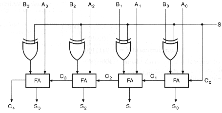
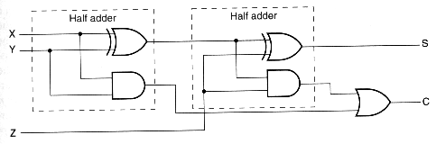
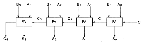
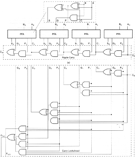
Now to subtract two numbers, we simply complement the minuend, and then simply add it to the subtrahend to give the appropriate result.

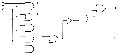
adder-subtractor circuit